市場データを読み込み中...
2026年7月23日木曜日
ホームへ戻るNews

SK Hynix Board Clears ₩7.09T for Cheongju P&T7 Packaging Hub — CEO Flags 2027 DRAM Supply Cliff

執筆 MinJeKim0 回閲覧

この記事の日本語訳は準備中です。以下は英語の原文です。

SK Hynix Board Clears ₩7.09T for Cheongju P&T7 Packaging Hub — CEO Flags 2027 DRAM Supply Cliff

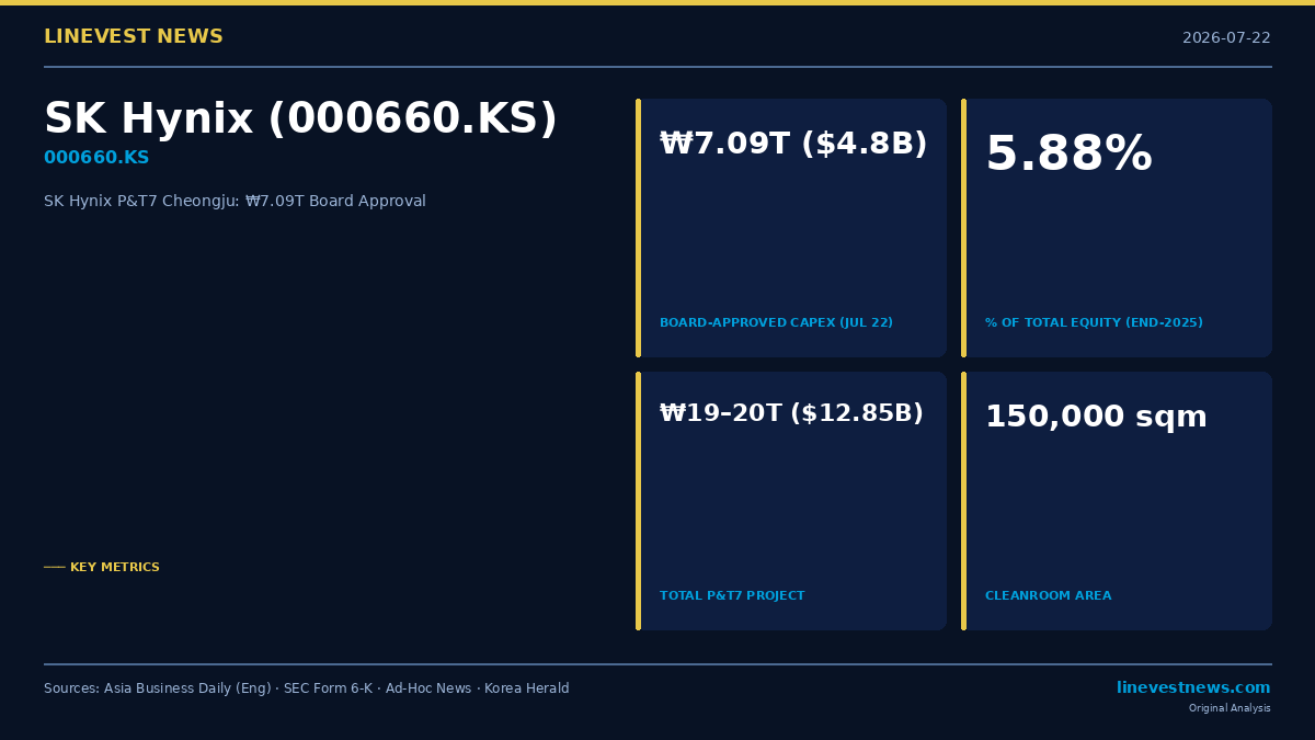
TL;DR - SK Hynix (000660.KS) board approved ₩7.0931T ($4.8B) for Cheongju P&T7 packaging facility on July 22 - Investment equals 5.88% of total equity; cleanroom opening accelerated vs. original schedule - Total P&T7 project: ₩19–20T ($12.85B), part of ₩100T Cheongju megaplan announced July 2 - CEO Kwak: DRAM supply meets only 75–80% of global demand; could fall to ~60% by 2027 - 2026 HBM output already sold out — back-end packaging is now the critical AI memory bottleneck


The Board Decision

SK Hynix (000660.KS) convened its board on July 22, 2026, and approved ₩7,093.1 billion ($4.8 billion at prevailing ₩1,480/USD) in capital for the construction and equipping of P&T7, its advanced packaging and test facility in Cheongju, North Chungcheong Province.

The approval — formally disclosed as a Form 6-K current report filed with the U.S. Securities and Exchange Commission — represents an increase from the previously budgeted figure, reflecting "increased production needs and an accelerated cleanroom opening schedule," the company stated. The ₩7.09T investment equals 5.88% of SK Hynix's total equity as recorded on December 31, 2025.

P&T7 is the company's dedicated back-end manufacturing complex situated in the Cheongju Techno Valley Industrial Complex. Construction formally commenced on November 26, 2025, with the original full-completion date set at December 31, 2032. The July 22 accelerated plan targets an earlier cleanroom handover within that window. At full buildout, P&T7 is designed to span approximately 150,000 square meters of cleanroom: roughly 60,000 sqm of wafer-level packaging (WLP) lines across three floors, and approximately 90,000 sqm of wafer test operations across seven floors.

The July 22 board vote marks the latest in a series of project milestones. In January 2026, SK Hynix first disclosed total P&T7 capital expenditure of approximately ₩19 trillion ($12.85 billion), making it one of the largest semiconductor packaging investments in history. In April 2026, CEO Kwak Noh-jung attended the groundbreaking ceremony. On July 2, 2026, he placed P&T7 inside the company's ₩100 trillion Cheongju commitment — ₩80 trillion for the M17 next-generation NAND fabrication plant (production targeting 1H 2029) and ₩20 trillion for P&T7 advanced packaging.


Why P&T7, and Why Now

The acceleration cannot be separated from a structural demand signal that SK Hynix's own leadership has flagged publicly. CEO Kwak has warned that the global DRAM market is currently supplying only 75–80% of aggregate demand, and that the shortfall could deepen to approximately 60% by 2027 unless significant new capacity comes online. SK Hynix entered 2026 with its entire high-bandwidth memory (HBM) production for the year already committed to customers, while enterprise B2B revenue — AI data-center orders for HBM and NAND — is projected to account for approximately 70% of total revenue across the 2026–2027 growth cycle.

The critical insight behind P&T7 is that the binding constraint has shifted. In the early phases of the HBM ramp, the primary bottleneck was producing underlying 1b-process DRAM wafers at sufficient volume. SK Hynix has progressively addressed that front-end constraint through capacity additions at M15X and related fab sites. Today, the new chokepoint is at the back end: taking individual DRAM dies, stacking them in the precise HBM architecture, performing thermal compression bonding at micro-scale, and executing wafer-level testing — all of which demand dedicated packaging infrastructure that is fundamentally distinct from standard DRAM production. P&T7 is purpose-built to remove that constraint.


Regional Context: A ₩392T Semiconductor Megaproject

P&T7 sits within a dramatically larger national commitment. On July 2, the government and Korea's leading chipmakers jointly announced ₩392 trillion ($252.5 billion) in total investment across the Chungcheong region:

CompanyCommitmentFocus Area
Samsung Electronics₩56THBM fab + advanced packaging
Samsung Display₩67TOLED and next-generation displays
Samsung SDI₩9TBattery manufacturing
SK Hynix (M17)₩80TNAND flash fab, 1H 2029 production target
SK Hynix (P&T7)₩20TAdvanced packaging hub, cleanroom 2027
AI data centers & others₩150T+Semiconductor ecosystem infrastructure

The ₩7.09T approved on July 22 represents an increase within the ₩20T P&T7 envelope — management is front-loading capital to pull the cleanroom handover date forward, rather than deferring to the 2032 full-completion timeline.


Investor Implications

The acceleration is a demand signal, not a supply-surplus reaction. SK Hynix does not accelerate $4.8 billion in packaging capex without customer commitments. The company's HBM4 order book — driven primarily by NVIDIA (Vera Rubin platform, commanding an estimated ~70% SK Hynix HBM4 share) and AMD (MI455X Helios platform, announced by Microsoft Azure on July 20) — provides multiyear revenue visibility that underwrites this outlay.

Packaging focus clarifies the competitive risk profile. Samsung Electronics (005930.KS) is investing ₩56T in Chungcheong HBM and packaging, and continues efforts to recover HBM4 market share after losing the NVIDIA Blackwell contract. Both companies will add packaging capacity, but SK Hynix's P&T7 is further along the construction timeline: groundbreaking occurred in April 2026, against Samsung's planned start later in the cycle.

Long amortization horizon warrants monitoring. ₩19–20T amortized over six to seven years of productive life represents a substantial fixed-cost base that will pressure free cash flow even as revenue scales. However, with the CEO indicating that the supply-demand gap may widen through 2027, HBM pricing is expected to remain firm enough to support margins sufficient to service the investment.

Regulatory and energy tailwinds. The government's ₩392T megaproject creates tax incentive alignment and political support for permitting and energy supply in Chungcheong, reducing execution risk relative to overseas competing sites.

Risk factors to monitor: - HBM revenue is heavily concentrated — approximately 75% traceable to NVIDIA alone. Any deceleration in AI data-center spending could leave P&T7 underutilized relative to the planned ramp. - The M17 NAND fab ramp (1H 2029) overlaps with the P&T7 packaging acceleration, creating concurrent capex peaks that will strain free cash flow through 2027–2028. - Foreign institutional investors registered a record net-sell day in SK Hynix on July 22 — the same session as the P&T7 board approval — suggesting the position unwind following the previous day's 6% KOSPI rally may temporarily separate near-term share price from the medium-term fundamental case.

Bottom line: The P&T7 acceleration confirms SK Hynix's management reads the HBM supply chain as structurally constrained, not cyclically tight. Back-end packaging is now the binding constraint on global AI memory output. The company is committing ₩7.09 trillion in a single board resolution to address it — a scale of capital commitment that is difficult to interpret as anything other than a multi-year demand confirmation.


This article is for informational purposes only and does not constitute investment advice. SK Hynix (000660.KS) is traded on the Korea Stock Exchange.

Sources: - SK hynix to Invest 7.0931 Trillion Won in Cheongju P&T7 Production Facility — Asia Business Daily (English) - SK hynix plans ₩7.09T AI memory plant investment | SEC Form 6-K — Stock Titan - SK Hynix Pours $5.8 Billion Into Korean Plant as CEO Flags 2027 Supply Crisis — Ad-Hoc News - Samsung, SK hynix to build HBM packaging fabs in Chungcheong region as part of ₩392T in total investment — Korea Herald - SK hynix Breaks Ground on P&T7 Advanced Packaging Fab in Cheongju — TrendForce - SK Hynix to invest $12.85bn in advanced packaging plant in Cheongju, South Korea — Data Center Dynamics

見出しの先を読む

何が起きたかは読みました。次は、それが何を意味するかを。

無料デイリーブリーフィング

韓国市場を毎朝 — 無料で

LineVest Dailyがソウル市場の寄付き前に届きます:KOSPI・KOSDAQの主要ストーリー、決算、開示、外国人フロー — わかりやすい英語で。無料、カード登録不要。

LineVest Dailyを無料で →
この企業

SK Hynixの詳細レポート

SK Hynixの最新DART開示を全て読み込みます — K-IFRSの財務、ガバナンス、株価への意味まで。3時間以内にPDFでお届け。

$12・買い切り

SK Hynixレポートを入手
ウォッチ銘柄すべて

市場全体をフォロー

週に何銘柄も韓国株を見ていますか?すべての分析記事を公開と同時に — デイリーのKOSPI・KOSDAQ全カバレッジと90日アーカイブ。

$9.99・月額

購読する

一次資料のDART開示に基づく独立ジャーナリズム — 投資助言ではありません。証券会社との提携はありません。