Samsung's Chip Division Caught Off Guard by Honam Fab Plan, Insiders Warn of Logistics Gaps and Cycle Risk
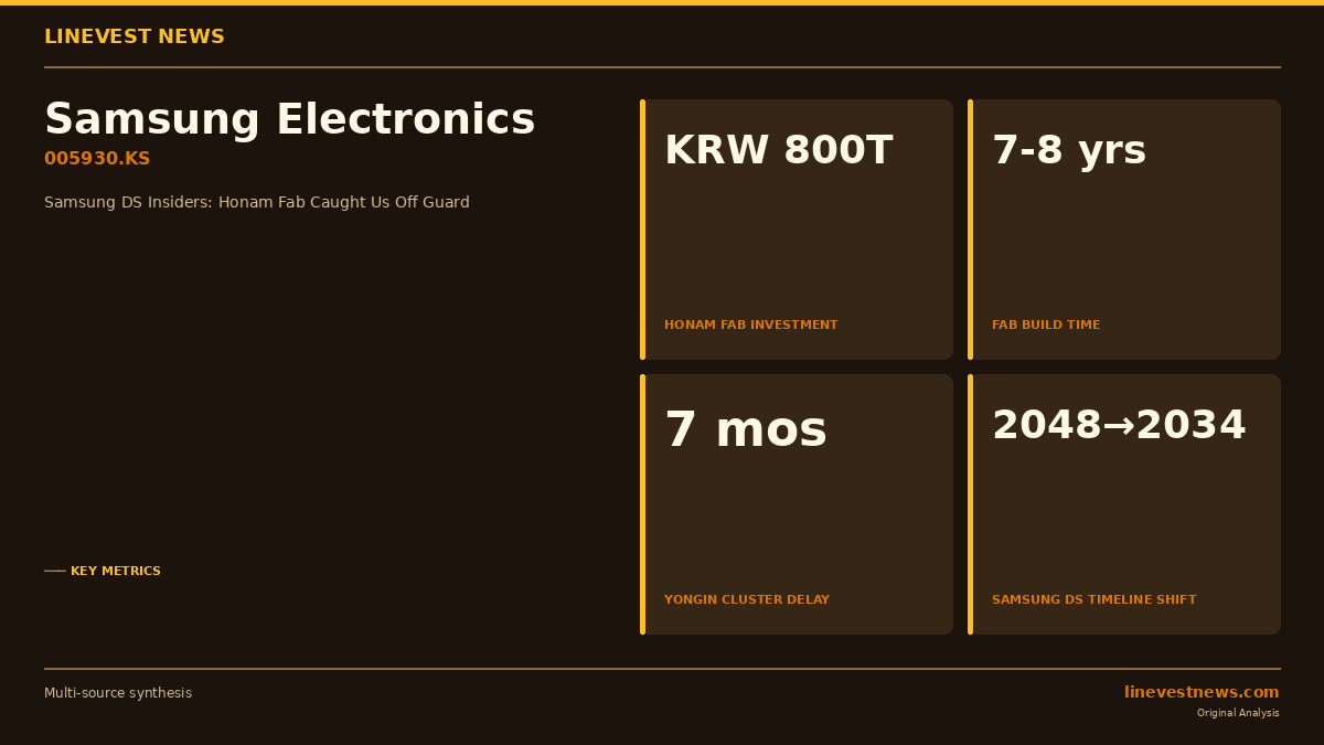
Samsung Electronics (005930.KS) publicly welcomed President Lee Jae-myung's KRW 800 trillion Honam semiconductor megaproject on June 29, but working-level executives inside the company's semiconductor (DS) division were reportedly blindsided — and are now grappling with how to fit a sprawling new fab network into a roadmap that was never designed around South Jeolla Province, multiple Samsung DS insiders told Chosun Biz.
What the Announcement Says vs. What Insiders Are Saying
At the Blue House ceremony, Chairman Lee Jae-yong committed to building two front-end fabs in Gwangju as part of a four-chipmaker cluster intended to rival Pyeongtaek and Yongin. The government's plan envisions pulling Samsung's long-range timeline forward by roughly 14 years — from a 2048 target date to 2034–35.
Publicly, Samsung DS said it has "no specific plans confirmed yet and therefore nothing additional to disclose."
Privately, it is a different story. A Samsung DS memory division executive told Chosun Biz: "Since this was not a directly intended investment, it will take time" to translate the announcement into an actionable blueprint. A second Samsung semiconductor official said the division had been uneasy about political pressure for a Honam fab since early Q1 2026, but "did not expect it to escalate to this scale." Some insiders went further, describing the announcement as "the worst thing we feared happening."
The Operational Bottlenecks Samsung Must Now Solve
The friction is structural, not political. Samsung DS already has three major Korean investment fronts in motion — none of which are fully resolved:
- Yongin National Industrial Complex: A public-private-government coordination panel has been deadlocked for seven months. Land compensation has not been completed. The first Yongin wafer line is not imminent.
- Pyeongtaek: Additional production-line expansions are still planned and being phased.
- Hwaseong: Serves as the company's core R&D and production-technology hub; key engineers are concentrated here.
Adding Honam to this picture forces Samsung to split limited capital expenditure and a finite pool of specialist engineers across at least three domestic super-sites simultaneously, insiders said.
There is also a physical logistics problem baked into the government's blueprint. The plan routes front-end wafer production through Gwangju (South Jeolla), then ships finished wafers to back-end packaging plants in Cheonan and Onyang (South Chungcheong Province), before the packaged chips travel to Incheon International Airport for export. By contrast, Samsung's existing Pyeongtaek campus is roughly 75 kilometres from Incheon — a fraction of the distance. Industry observers note the multi-hop supply chain is logistically inefficient by semiconductor-industry standards and adds cost variability that Samsung's current facilities do not face.
The Cycle Risk the Government Isn't Talking About
Government officials justified the accelerated timeline by pointing to surging AI-driven memory demand. But industry analysts are pushing back on the assumption that the current super-cycle will still be running when Honam fabs are ready.
A single leading-edge semiconductor fabrication plant takes seven to eight years to design, permit, build, equip, and qualify. That puts initial Honam wafer output no earlier than approximately 2033–2034. Industry participants note that if a memory-market peak-out — a widely discussed scenario for post-2027 — materialises, the demand environment when Honam fabs begin shipping chips could look substantially different from today's AI-boom conditions.
"Finding people willing to relocate to Yongin and Pyeongtaek is already difficult," one industry contact told Chosun Biz. "Splitting the workforce further toward Honam — and then adding the possibility of enormous losses if the market enters oversupply — means too many risk factors to count."
Investor Takeaway
For Samsung Electronics shareholders, the announcement introduces a set of risks that the company's official communications have not fully articulated:
- Capex overextension: Committing to simultaneous Gwangju (front-end) + Cheonan/Onyang (back-end) + Yongin + Pyeongtaek expansions increases the probability of cost overruns and delayed returns.
- Talent dispersion: Korea's pool of advanced semiconductor process engineers is finite; splitting it across more sites risks slowing qualification timelines at every location.
- Cycle timing mismatch: A fab announced in 2026 and breaking ground in 2027 that takes 7–8 years to complete is a 2034–35 asset. Investors must assess whether memory demand in 2034 will justify the cost basis.
- Technology lock-in: Once construction begins, switching the process node or architecture of a wafer fab mid-construction is extraordinarily expensive. Government-driven announcements that front-run detailed commercial planning limit Samsung DS's flexibility to adapt to evolving customer specifications — HBM generations, process nodes, NAND vs. DRAM mix.
Samsung Electronics has yet to publish a revised capex schedule, and the Blue House has not indicated which government body will coordinate site selection, infrastructure, and regulatory approvals for a project of this scale.
Sources: Chosun Biz · Newsis Economy · ETNews