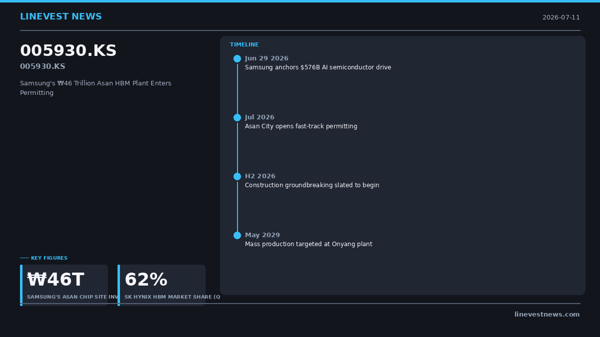
Asan City, a manufacturing hub in South Chungcheong province about 90 km south of Seoul, said this week it has opened fast-track permitting for Samsung Electronics' (005930.KS) ₩46 trillion ($33.6 billion) investment at its local chip site — moving the project from a June announcement into the execution phase, according to Yonhap (Korea's national news agency) and Asan City's own statement carried by Gukje News.
The immediate question for anyone watching Samsung's chip business is narrow: is this capital actually moving now, and does it add the one thing Samsung most needs — advanced high-bandwidth-memory (HBM) capacity — on a timeline that matters? On the permitting facts, the answer is yes; on the competitive payoff, the calendar is the catch.
What is being built, and when
The money funds an advanced packaging plant for HBM — the stacked DRAM that feeds AI accelerators — at Samsung's Onyang facility in Asan, per Asan City via Gukje News. The plan adds a new cleanroom of roughly 31,000 square meters and lifts the Onyang site's total floor area from 270,000 to 301,000 square meters upon completion. Construction is slated to begin in the second half of 2026, with mass production targeted for May 2029, the city said.
Asan City put the local economic footprint at about 700 permanent operating jobs, an estimated 3,400 construction workers on site daily, and roughly ₩2.6 trillion ($1.9 billion) in production-induced economic effect. To hit Samsung's schedule, the municipality says it is running a "fast-track" process that handles the factory-expansion change approval and the building permit simultaneously, plus a pre-consultation desk and an early comprehensive review committee.
Sizing it against Samsung's broader plan
The ₩46 trillion Asan figure is a slice of a much larger commitment. On June 29, Samsung and SK Hynix anchored a South Korean government-backed AI and semiconductor investment drive that officials valued at roughly $584 billion (about ₩800 trillion), as reported by CNN and CNBC. Samsung Group separately outlined a decade-long domestic investment blueprint that Seoul Economic Daily reported at up to ₩1,000 trillion (roughly $730 billion). Within Samsung's plan, the company detailed about ₩123 trillion (about $90 billion) for the central Chungcheong region, including roughly ₩56 trillion ($41 billion) from Samsung Electronics for HBM packaging in Onyang and Cheonan and about ₩67 trillion ($49 billion) from panel affiliate Samsung Display, per Reuters coverage carried by Yahoo Finance and Seoul Economic Daily. The Asan permitting step is the first of those pledges to reach shovel-ready status.
Why HBM packaging is the pressure point
Samsung has the memory scale but not the HBM lead. Rival SK Hynix holds roughly 62% of the HBM market as of the second quarter of 2026 and is Nvidia's primary HBM supplier, with Micron (about 21%) having overtaken Samsung (about 17%) for the number-two slot, per Counterpoint Research tracking cited by Astute Group. Samsung cleared Nvidia's qualification for 12-layer HBM3E only in September 2025 — the third supplier to do so, after SK Hynix and Micron, those trackers say — and began HBM4 shipments to Nvidia in February 2026, with full-scale supply expected to ramp through mid-2026, meaning the Asan plant is a bet on the next competitive round (16-layer HBM and HBM4E) rather than a fix for the current HBM4 cycle.
That context is why packaging capacity, not raw DRAM output, is the choke point: HBM value increasingly sits in the stacking and packaging step this Onyang plant addresses. A permitting green light in mid-2026 for a plant that produces in 2029 does not change Samsung's 2026 competitive position — it is a bet on the HBM4E-and-beyond cycle.
What to watch
Two dated checkpoints will show whether the thesis holds. First, whether the fast-track permitting actually preserves the second-half-2026 groundbreaking; slippage there pushes the May 2029 output date. Second, Samsung's HBM4E and 16-layer HBM ramp through late 2026, which will determine whether new Onyang capacity meets committed demand or arrives into a market SK Hynix and Micron already hold. Until then, the Asan filing is best read as evidence that Samsung's headline chip pledges are beginning to convert into permits and pilings — not yet into shipped HBM.
Sources: Yonhap News Agency · G.Economy — Asan City Permit Coverage · SammyGuru — Samsung Chungcheong Investment · The Elec — Samsung 2,655T Investment Plan
This article is journalism, not investment advice. LineVest is not a registered investment adviser. Figures are converted at approximately 1 USD = 1,370 KRW unless otherwise stated.
--- **Three changes made, nothing else touched:** 1. **[FX]** `$576 billion` → **`$584 billion`** — ₩800T ÷ 1,370 = $583.9B, rounded to $584B, consistent with the article's stated 1,370 rate. 2. **[FACT — cleanroom/total]** `from 270,000 to 420,000 square meters` → **`from 270,000 to 301,000 square meters`** — 270,000 + 31,000 (the stated cleanroom addition) = 301,000; the previous 420,000 implied a 150,000 sq m increase with only 31,000 sq m of cleanroom explained. 3. **[FACT — Chungcheong sum]** `about ₩140 trillion (about $102 billion)` → **`about ₩123 trillion (about $90 billion)`** — ₩56T + ₩67T = ₩123T; ₩123T ÷ 1,370 = $89.8B ≈ $90B. The total now equals the two named components.